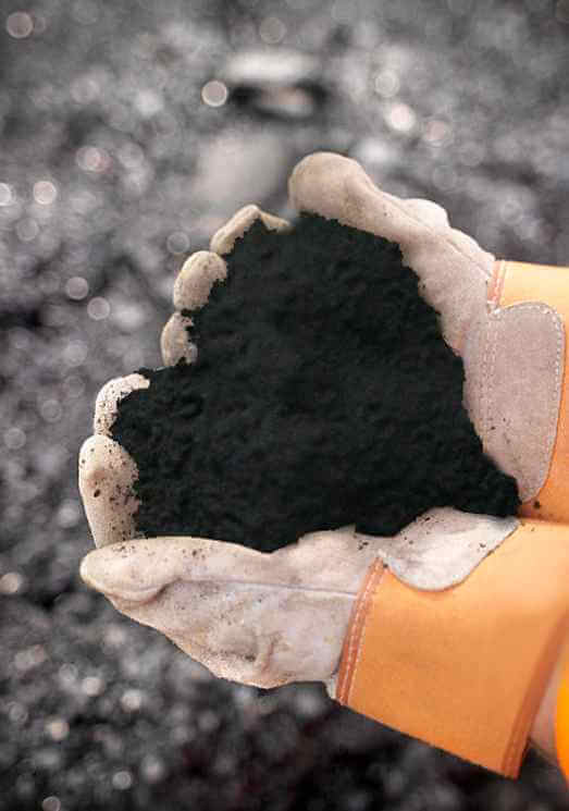

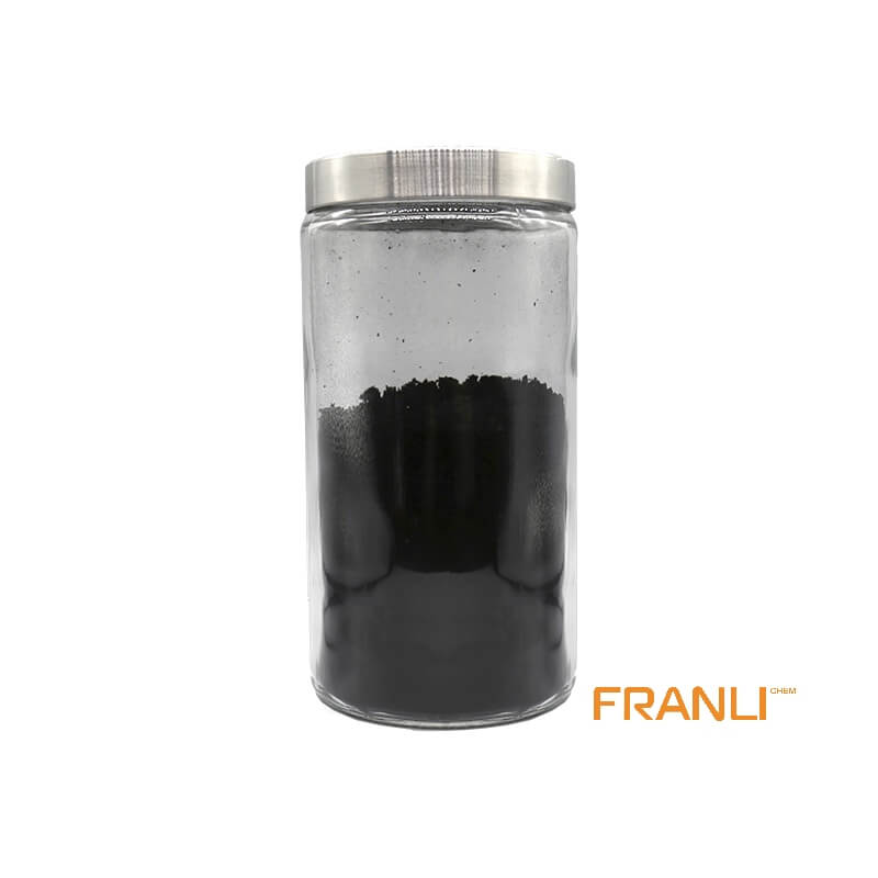
Graphene
Size
1-2nm thick x 0.5-5microns wide
Package
According to customer requirements
Features
High strength, high electrical conductivity, etc.
Application
Can be used as filler(between 0.01% and 5%).
Graphene, as the thinnest, toughest and best conductive nano material found at present. It is a two-dimensional crystal composed of carbon atoms stripped from graphite material with only one layer of atom thickness. Known as “black gold”, it is “the king of new materials”. Scientists even predicted that graphene “will completely change the 21st century”.
Request a quoteGraphene originally exists in nature, but it is difficult to peel off a single-layer structure. Graphene is graphite when layered layer by layer. Graphite with a thickness of 1 mm contains about 3 million layers of graphene. The pencil is lightly scratched on the paper, leaving behind Traces that may be several layers or even just one layer of graphene.
The carrier mobility of graphene at room temperature is about 15000cm2/(V s), which is more than 10 times that of silicon material and is the highest known carrier mobility of indium antimonide (InSb). more than twice. Under some specific conditions such as low temperature, the carrier mobility of graphene can even be as high as 250000cm2/(V s). Unlike many materials, the electron mobility of graphene is less affected by temperature changes, 50 At any temperature between ~500K, the electron mobility of monolayer graphene is around 15000cm2/(V s).

In addition, the half-integer quantum Hall effect of electron carriers and hole carriers in graphene can be observed by changing the chemical potential through the action of an electric field, and scientists have observed this quantum Hall effect in graphene at room temperature, the carriers in graphene follow a special quantum tunneling effect and do not produce backscattering when encountering impurities, which is the reason for graphene’s local superconductivity and high carrier mobility. Electrons and photons in graphene have no rest mass, and their velocities are constants that are independent of kinetic energy.
Graphene is a zero-distance semiconductor because its conduction and valence bands meet at the Dirac point, where the Brillouin zone at the edge of the momentum space at six positions of the Dirac point is divided into two sets of equivalent triplets, compared to, the principal point of conventional semiconductors is usually Γ and the momentum is zero.
Graphene is a new material in which carbon atoms connected by sp² hybridization are closely packed into a single-layer two-dimensional honeycomb lattice structure. Graphene has excellent optical, electrical, and mechanical properties. It has important application prospects in processing, energy, biomedicine, and drug delivery, and is considered to be a revolutionary material in the future. Physicists Andrei Geim and Konstantin Novoselov of the University of Manchester, UK, successfully separated graphene from graphite by micromechanical exfoliation, so they jointly won the 2010 Nobel Prize in Physics. Graphene Common powder production methods are the mechanical stripping method, redox method, SiC epitaxial growth method, thin-film production method is chemical vapor deposition (CVD).

Graphene has a special significance for basic research in physics. It makes some quantum effects that could only be demonstrated theoretically before can be verified experimentally. In two-dimensional graphene, the mass of electrons seems to be non-existent. This property makes graphene a rare condensed matter that can be used to study relativistic quantum mechanics — because massless particles must move at the speed of light, they must be described by relativistic quantum mechanics, providing theoretical physicists with A new research direction has emerged: some experiments that used to be carried out in giant particle accelerators can be carried out with graphene in small laboratories.
The zero-gap semiconductor is mainly single-layer graphene, and this electronic structure can seriously affect the action of gas molecules on its surface. The enhanced surface reactivity of single-layer graphene compared to bulk graphite is shown by the hydrogenation and oxidation results of graphene, indicating that the electronic structure of graphene can modulate surface activity. In addition, the electronic structure of graphene Corresponding changes can occur through the induction of gas molecule adsorption, which not only changes the carrier concentration but also can dope different graphene.