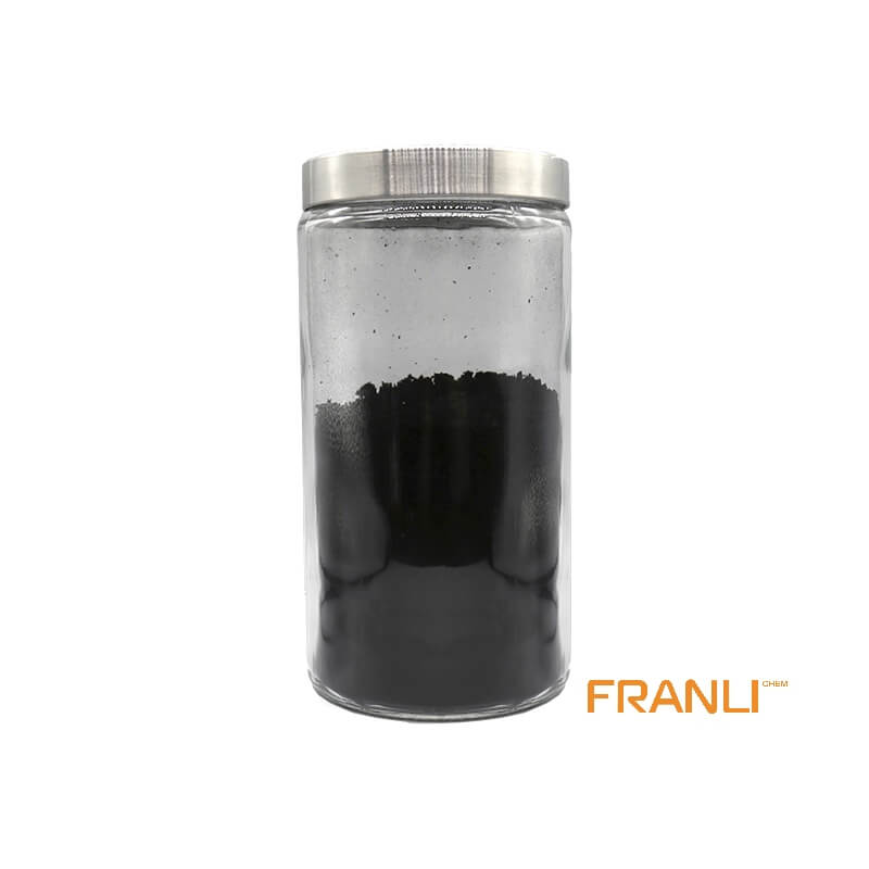
Graphene
Size
1-2nm thick x 0.5-5microns wide
Package
According to customer requirements
Features
High strength, high electrical conductivity, etc.
Application
Can be used as filler(between 0.01% and 5%).
Graphene, as the thinnest, toughest and best conductive nano material found at present. It is a two-dimensional crystal composed of carbon atoms stripped from graphite material with only one layer of atom thickness. Known as “black gold”, it is “the king of new materials”. Scientists even predicted that graphene “will completely change the 21st century”.
Request a quote
With the increasing use of graphene in many applications, the market demand for graphene has been rising in the past few years. This has further promoted the research work behind graphene synthesis methods, one of which is chemical vapor deposition (CVD). In this article, we will introduce how a research team uses simulation to analyze and enhance the growth mechanism of CVD graphene.
You may have heard the word “graphene” in the news. Of course, you may have read it many times in our articles. Reports generally mention their great role in promoting technological progress in various industries. We do not find unique and powerful materials like graphene every day. Now we can confidently say that the world has noticed this material.

Graphene is a topic related to many people, including ourselves. In a recent article series, we highlighted the revolution behind this material, from its properties and production methods to simulating its use in various applications.
In the last article of this series, we emphasized the research work of “magic material”, which helped us inadvertently discover the material of two-dimensional glass. Although the material discovery itself is a great achievement, here I would like to focus on the graphene growth method used in their research, namely chemical vapor deposition (CVD).
Chemical vapor deposition describes a chemical process designed to produce high-purity solid materials with high strength. In this method, gas molecules are bonded together in a reaction chamber containing a heated substrate. The interaction between the gas and the heated substrate causes the gas to react and/or decompose on the substrate surface, to produce a material film.

This synthesis method can produce quite high-quality materials, so it is very useful. Compared with other coating methods, the materials obtained in chemical vapor deposition often have higher purity and hardness and are more earthquake-resistant or damage resistant. Another advantage of this method is that it can deposit a variety of materials, one of which is graphene.
Among various synthesis technologies, chemical vapor deposition has been proved to have broad prospects in the development of high-quality graphene films. This process refers to the growth of graphene films, such as nickel (Ni), on different substrates made of transition metals. This involves the diffusion of decomposed carbon atoms into nickel at high temperatures and the precipitation of carbon atoms on the surface of nickel during cooling.
Due to the diversity of growth conditions in the CVD method, the production of monolayer graphene and the control of graphene film quality become quite challenging. A research team at the University of Arkansas recognized the need to better understand the growth mechanism of graphene and the optimal conditions for graphene production.

