Graphene
Size
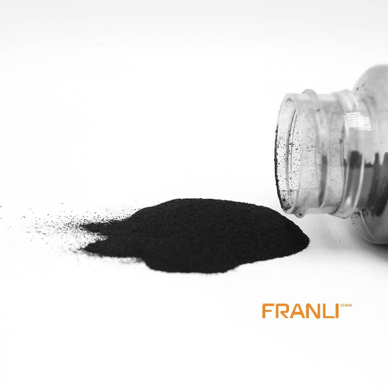
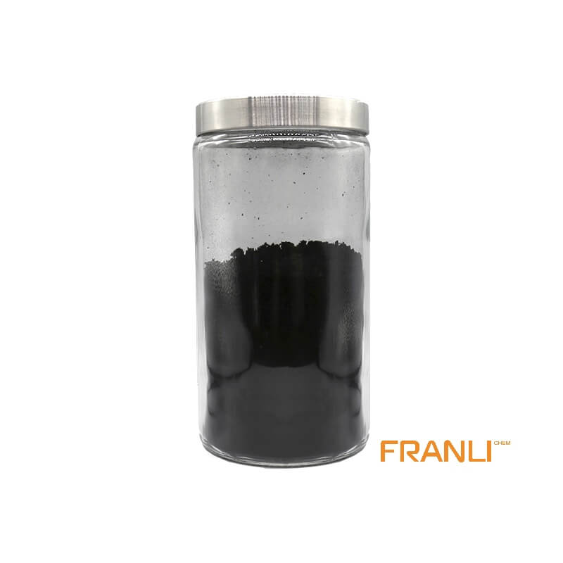
1-2nm thick x 0.5-5microns wide
Package
According to customer requirements
Features
High strength, high electrical conductivity, etc.
Application
Can be used as filler(between 0.01% and 5%).
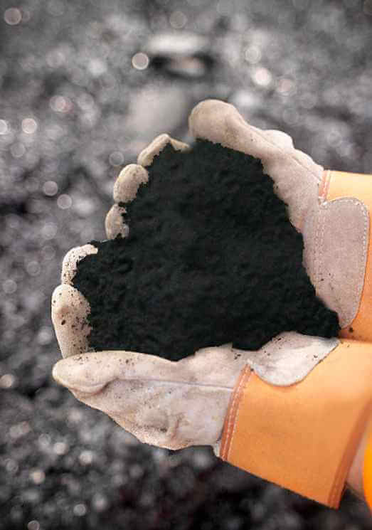
Graphene, as the thinnest, toughest and best conductive nano material found at present. It is a two-dimensional crystal composed of carbon atoms stripped from graphite material with only one layer of atom thickness. Known as “black gold”, it is “the king of new materials”. Scientists even predicted that graphene “will completely change the 21st century”.
Request a quote
Graphene is a kind of ² Hybrid connected carbon atoms that are closely packed into a single-layer two-dimensional honeycomb lattice structure. Graphene has excellent optical, electrical, and mechanical properties. It has important application prospects in materials science, micro-nano processing, energy, biomedicine, and drug delivery. It is considered to be a revolutionary material in the future. physicists Andre Geim and Konstantin Novoselov from the University of Manchester, UK, successfully separated graphene from graphite by micromechanical stripping method, so they jointly won the 2010 Nobel prize in physics. The common powder production methods of graphene are the mechanical stripping method, redox method, and SiC epitaxial growth method, and the film production method is the chemical vapor deposition method.

Graphene is one of the materials with the highest strength known. At the same time, it also has good toughness and can be bent. The theoretical Young’s modulus of graphene is 1.0tpa and the inherent tensile strength is 130gpa. The reduced graphene modified by hydrogen plasma also has very good strength, and the average modulus can be greater than 0.25 TPA. The graphite paper composed of graphene flakes has many holes, so the graphite paper looks very brittle. However, the functional fossil graphene is obtained by oxidation, and then the graphite paper made of functional fossil graphene will be extremely strong and tough.
Graphene has very good thermal conductivity. The thermal conductivity of pure defect-free single-layer graphene is as high as 5300w / MK, which is the highest carbon material by far, higher than that of single-walled carbon nanotubes (3500W / MK) and multi-walled carbon nanotubes (3000W / MK). When it is used as a carrier, the thermal conductivity can also reach 600W / MK. In addition, the ballistic thermal conductivity of graphene can move down the lower limit of the ballistic thermal conductivity of carbon nanotubes per unit circumference and length.

Graphene has very good optical properties, and its absorption rate is about 2.3% in a wide wavelength range. It looks almost transparent. Within the thickness range of several layers of graphene, the absorption rate increases by 2.3% for each additional layer. Large area graphene films also have excellent optical properties, and their optical properties change with the change of graphene thickness. This is the unusual low-energy electronic structure of single-layer graphene. When a voltage is applied to the double gate double-layer graphene field-effect transistor at room temperature, the bandgap of graphene can be adjusted between 0 ~ 0.25eV. When a magnetic field is applied, the optical response of graphene nanoribbons can be tuned to the terahertz range.
Franli can provide 2-5 layers of graphene with a content of more than 99% and an average thickness of 1-2nm. If you are interested, please contact us.

